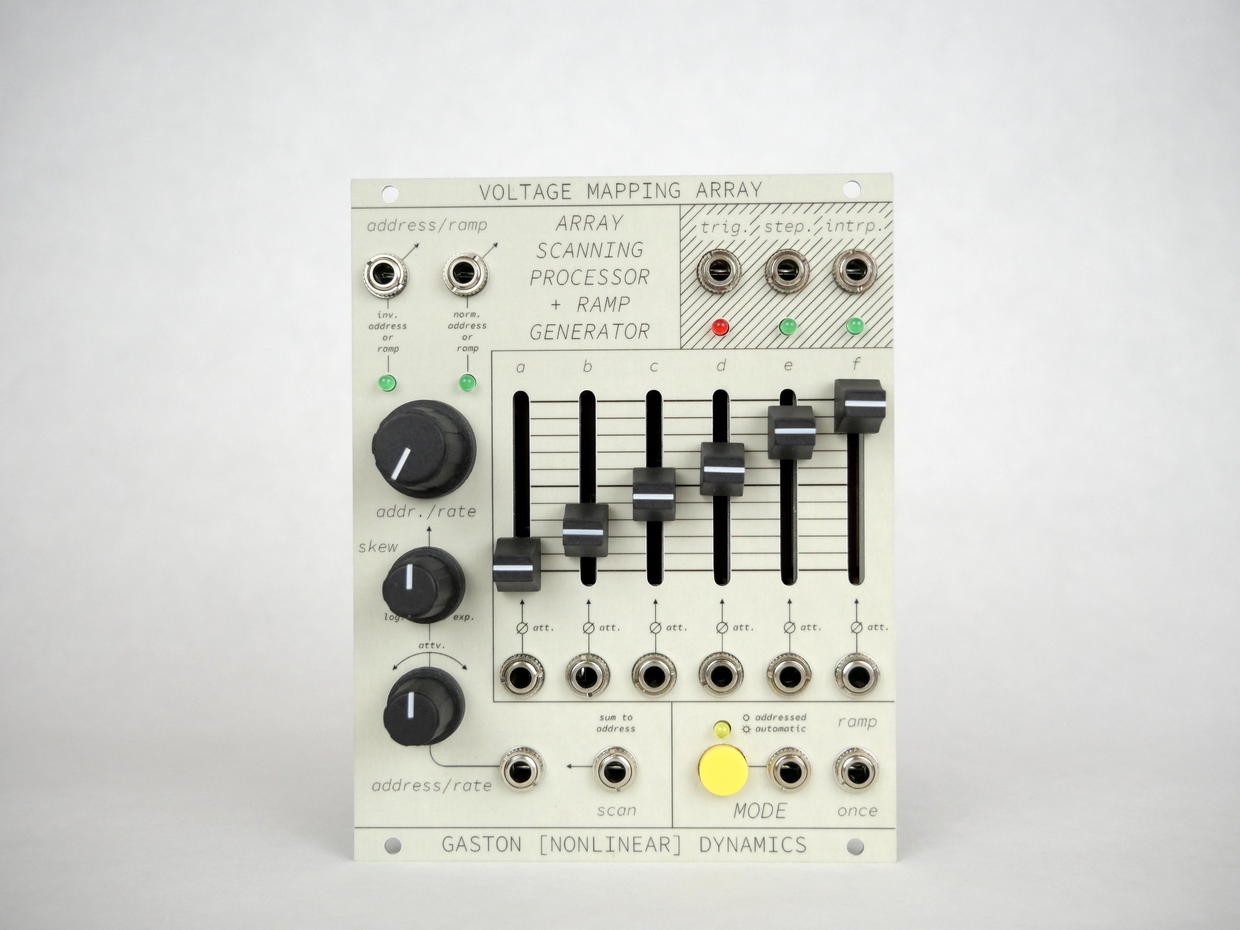
Voltage Mapping Array (2025)
Voltage Mapping Array prototype
Voltage Mapping Array is a general-purpose control voltage generator + processor for the [Nonlinear] Dynamics system. It may be used for a variety of purposes, including nonlinear control voltage amplitude remapping, signal scaling, curve shaping, signal mixing, voltage-controlled scanning/crossfading/switching, attenuation, inversion, control voltage wrapping/folding, signal level comparisons, ramp generation, burst generation, crude envelope generation, tendency mask generation, null range/boundary definition, and more.
Voltage Mapping Array is based on a concept I’d hoped to build for years; I have notebooks with early sketches dating from 2018, around the time I first started working with prototypes of what would become Continual Transition. As I occasionally dove into new design projects and scoped out new development processes/platforms, the idea of this style of nonlinear control information processor was almost always one of the first ideas I wanted to build—however, I never actually built it until I started working with [gen~] and the Electrosmith Daisy Patch submodule.

An early testing setup for the [Nonlinear] Dynamics system, with two V1 Voltage Mapping Arrays (top left), as well as a Test, two Destabilized Impulse Generators, and the first Audio Combine.
Having had the concept for its core functionality in place for years, it was one of the first ideas I implemented using the PatchSM. Once I sat down to work on it in the summer of 2024, the [gen~] patch came together in a couple of hours. I did the layout and graphics for the first hardware prototype that summer, and built the (first and only) two V1 units in September of 2024.
As new modules came into being, I gradually narrowed in on a clearer sense of the desired ergonomics of the system as a whole. I redesigned the module in December 2024/January 2025, reducing its size and considerably expanding its functionality.
The array: Addressed Mode
Voltage Mapping Array is perhaps best understood as a means of defining an arbitrary distortion process for control signals. One can think of the six slide potentiometers as representing six breakpoints in an amplitude remapping transfer function. The module offers two Modes, switchable using a dedicated yellow tactile switch and corresponding trigger input. The two modes are Addressed and Automatic; we will begin by discussing Addressed mode.
Consider a control signal to the scan input. 0V at the scan input will produce the a slider value at the interp. (interpolated) output; 5V at the scan input will produce the f value at the interp. output. Intermediate incoming amplitude values will produce an output voltage corresponding to the respective position along the “graph” of the six breakpoints. So, by arranging the six sliders in ascending order (as seen in the photograph above), a near 1:1 relationship between input and output is possible; more unusual arrangements will result in more unusual relationships between the input and output signals.
One obvious use is to reshape any of the [Nonlinear] Dynamics system’s many ramp generators. Simply plug a ramp generator (from Trajectory Generator, 4-D Input Port, or another Voltage Mapping Array) into the scan input. The interp. output will produce a distorted version of the ramp, which will assume the shape of the sliders on the panel.
Aside from the obvious interesting and non-specific use case of converting control voltages into more peculiar control voltages, this presents several important opportunities. For instance, consider a scenario in which a, b, and c are set to their minimum position, and d, e, and f are arranged in gradually ascending order, with f at its maximum value. This transfer function is an example of null range/boundary definition (and an appropriate complementary voltage range expansion). Incoming signals below ~2.5V will produce 0V at the interp. output. Signals between 2.5V and 5V will be linearly remapped to the range of 0V to 5V. This transfer function produces an output voltage range identical to its input, but ignores voltages below 2.5V and expands the range of voltages above 2.5V, effectively making it such that incoming modulation doesn’t “kick in” until this (arbitrary) threshold has been breached. This technique finds particular utility in concert with gestural control sources—for instance, allowing the fine-tuning of pressure curves, etc.
The stepped or step. output behaves similarly; however, it lacks the interp. output’s linear interpolation—discretely switching between the slider array’s values rather than continuously fading between them. The trigger or trig. output produces a momentary trigger each time the stepped output changes value.
In Addressed mode, the large addr./rate knob can be used to manually address the array. This can be useful for fine-tuning values in the array, or as a performance technique.

Address Folding
It is worth noting that, in Addressed mode, the address knob, address input, and scan input are all summed in order to address the array. Each of these controls can potentially span the entire array. In order to present interesting opportunities—and to avoid scenarios in which incoming signals cause the processor to “clip” at either end of the array—Voltage Mapping Array is capable of folding summed address signals that would otherwise breach “beyond” the a or f stages. Let’s consider each of these three control sources to have a “range” of 0–1 (corresponding to control voltages in the range of 0–5V). If the address knob is at 0.5 and the scan input at 0.75, the sum (1.25) exceeds the acceptable 0–1 range. This is resolved by subtracting the overflow from the 1 “boundary”—resulting in an address/position of 0.75. The same style of folding occurs at the “beginning” of the array as well: applying a negative offset to the address via the address input and attenuverter can cause the final address to “fold” or “reflect” upward.
The folding feature can be useful for various voltage processing techniques, ranging from basic signal inversion to dynamic direction changes and more.
The Array: Automatic Mode
When switching to Automatic mode, Voltage Mapping Array engages an internal ramp generator. In Addressed mode, the large front-panel knob assumes its function as a rate control; likewise, the address/rate input and attenuverter provide voltage control of the ramp generator’s frequency.
The ramp generator assumes the role of a continuous array addressing function—scanning the full array from left to right. As such, Voltage Mapping Array may be used as a looping function generator with variable wave shape; likewise, it may be used as a six-stage control voltage/trigger sequencer.
Note that the scan input always acts as an address control; when in Automatic mode, this essentially amounts to phase modulation of the automatic voltage function.
Ramps
Voltage Mapping Array is capable of both processing and producing ramps. The utility of the two ramp outputs on the top left of the panel is most obvious when in Automatic mode. In this mode, with no signals applied to the scan input, the Normal Address or Ramp output produces an ascending ramp; the Inverted Address or Ramp output produces a descending ramp.

The instantaneous voltage levels at these outputs correspond to the current address; as such, their amplitude is affected by the internal ramp generator, scan input, and, when in Addressed mode, the address knob and CV input. As such, the Address/Ramp outputs can be used for a number of utility functions, ranging from signal mixing and voltage inversion to various other types of range remapping—all without requiring use of the mapping array itself.
Of course, in automatic mode, the ramp signals can be used as timing signals, or as sources for further nonlinear processing. One interesting application is to “link” two Voltage Mapping Arrays by setting one to Automatic mode and the other to Addressed mode. By connecting the Normal Address or Ramp output of the Automatic unit to the scan input of the Addressed unit, you can create relatively synchronous types of voltage movement.
Signal Routing
I have referred to Voltage Mapping Array as a many-to-one crossfader/switcher, and yet, all of the examples I have mentioned so far treat its individual breakpoints as more or less static values. Note that the jacks located below each breakpoint are control voltage inputs; when any of these is patched, it overrides a normalled connection from a 5V reference signal to the associated slide potentiometer, in essence turning the slider into an attenuator for the external input. In this way, it is possible to pass external signals to the interpolated or stepped outputs. You may also choose to think of this process as “modulating the breakpoint values,” but I’m inclined to point out that that is not the only perspective you may adopt.
So, you may consider Voltage Mapping Array to be a many-to-one crossfader/switch. The stepped output will select discretely between the six inputs, while the interpolated output will produce an interpolated mix of signals patched to the individual breakpoint CV inputs. Of course, modulating the address (or using Automatic mode) while dynamic signals are patched into the CV inputs turns Voltage Mapping Array into a many-dimensional processor, capable of many unusual functions.
Additional Notes
I have not yet mentioned the jack at the bottom right of the panel, labeled ramp once—and for good reason: its implementation is questionable, and I’m not yet confident that it offers any useful utility. Suffice it to say that when a signal is detected at this input (usually a signal with a hard rising edge), the internal ramp generator is engaged for a single cycle, at a rate determined by the address/rate knob and CV input (indeed, it basically sets the module to “Automatic” mode for a single cycle of the ramp generator). This can be used for crude triggered function generation, however, note that the address will always reset to the address represented by the address knob, CV input, and scan input upon completion of the automated ramp. It’s possible that you will find this useful. It’s possible that I will find another way to use this input. It’s possible that I will make a new version of this module that frees up that panel space for a more useful features.
Voltage Mapping Array is a concept/prototype developed primarily for personal use and is not available for purchase.